In the realm of electronics manufacturing, where precision and attention to detail are paramount, the tools we employ can determine the difference between a flawless product and costly rework. In this high-tech landscape, binocular and trinocular microscopes, alongside the ever-evolving realm of digital and hybrid systems, have emerged as essential assets. These instruments are at the heart of a quality assurance program that scrutinizes the intricate world of Printed Circuit Boards (PCBs) and electronic components.
In this article, we will explore the nuances that set binocular and trinocular microscopes apart, and how the digital revolution in imaging has not only changed the game but rewritten the rules on the production floor. We will also look at the IPC-A-610 standard and how it impacts the inspection process. Electronics manufacturing demands high precision and quality control, making microscopy an essential tool for inspecting various components and ensuring product reliability.
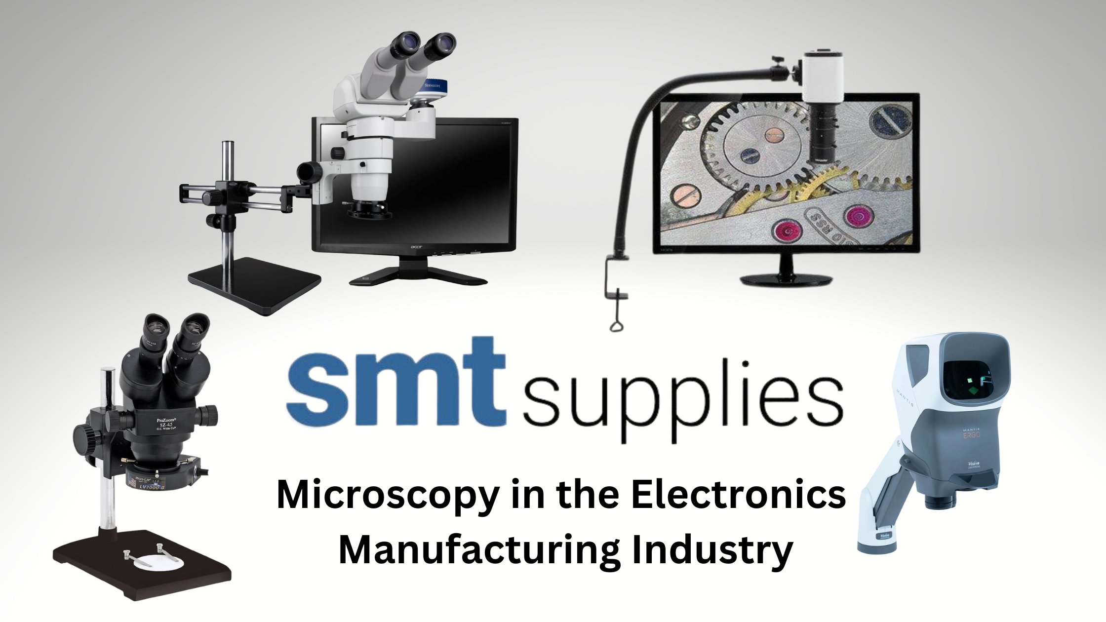
Binocular Microscopes
Binocular microscopes play a crucial role in the electronics industry, especially when inspecting Printed Circuit Boards (PCBs). There are many benefits to using binocular microscopes for this purpose:
- Enhanced Depth Perception: Binocular microscopes provide a three-dimensional view of the object being inspected. This depth perception helps technicians and engineers to accurately gauge the height differences between components on the PCB, aiding in identifying soldering defects, misalignments, and other issues.
- Improved Comfort: The new generation of Binocular microscopes are designed for extended use, reducing strain on the eyes and neck compared to single-lens microscopes. Operators can comfortably view and inspect PCBs for longer periods, leading to higher productivity and accuracy.
- Better Magnification Options: Binocular microscopes often offer a range of magnification options, allowing operators to switch between different levels of magnification for different inspection tasks. This versatility is especially important when examining intricate details on small components.
- Precise Solder Joint Rework, Touchup, and Inspection: PCBs have numerous solder joints that connect components to the board. Binocular microscopes enable operators to conduct precise hand soldering functions and inspectors to closely examine these solder joints for defects such as solder bridges, cold solder joints, and insufficient soldering. This level of precision helps to ensure the reliability and functionality of the final electronic product.
- Fine Component Inspection: Many electronic components, such as surface-mount devices (SMDs), are extremely small and require high magnification to be properly inspected. Binocular microscopes allow inspectors to focus on these tiny components, ensuring their correct placement and soldering.
- Defect Detection: Binocular microscopes enable operators to identify various defects, including hairline cracks, damaged traces, and component misalignments, which might not be visible to the naked eye. Detecting these defects early in the manufacturing process helps prevent costly rework and improves product quality.
- Quality Control: Binocular microscopes are essential tools for quality control processes in the electronics industry. They help ensure that PCBs meet industry standards and specifications, reducing the likelihood of faulty products reaching customers.
- Flexible Lighting Options: Many binocular microscopes come equipped with various lighting options, including adjustable LED lights and darkfield illumination. These lighting options enhance the visibility of different features on the PCB and allow for better contrast during inspections.
Binocular microscopes offer a range of benefits when inspecting PCBs in the electronics industry. They provide improved depth perception, comfort, magnification options, and precision, all of which contribute to better defect detection, quality control, and overall manufacturing efficiency.
Trinocular Microscopes
Trinocular microscopes, like binocular microscopes, are valuable tools in the electronics industry, particularly for inspecting Printed Circuit Boards (PCBs). Here are the benefits of using trinocular microscopes for this specific purpose:
- Simultaneous Observation and Documentation: Trinocular microscopes come equipped with a third viewing port (trinocular head) that allows for the attachment of a camera or imaging system. This feature enables operators to observe the PCB while simultaneously capturing images or videos of the inspection process. These images are invaluable for documentation, quality control, and collaboration among teams.
- Remote Collaboration: Trinocular microscopes with imaging capabilities enable remote collaboration. Engineers and colleagues can view real-time images of the inspection process from different locations, providing an opportunity for immediate feedback and decision-making without physically being present in the inspection area.
- Archiving and Analysis: The images and videos captured using trinocular microscopes can be archived for future reference. This is particularly useful for analyzing defects, identifying patterns, and improving inspection processes over time.
- Training and Education: Trinocular microscopes are excellent tools for training new personnel. Instructors can use the imaging capabilities to guide trainees through the inspection process and point out specific details to look for on PCBs. Trainees can also review recorded images as part of their learning process.
- Comparative Analysis: Trinocular microscopes allow inspectors to compare images of different PCBs or different sections of the same PCB. This capability is valuable for identifying variations, defects, or improvements across different production batches or designs.
- Accurate Reporting: The visual documentation produced by trinocular microscopes enhances the accuracy of inspection reports. Instead of relying solely on written descriptions, inspectors can include high-quality images and annotations that provide a clear visual representation of the inspected areas.
- Process Improvement: The ability to closely document and analyze PCBs using trinocular microscopes contributes to process improvement. By identifying recurring defects and their causes, manufacturers can adjust their processes to minimize defects and increase overall efficiency.
- Comprehensive Record Keeping: Trinocular microscopes support comprehensive record keeping by providing visual evidence of the inspection process. This is particularly important for meeting regulatory requirements and maintaining product traceability.
In summary, trinocular microscopes offer all the benefits of binocular microscopes while adding the significant advantage of integrated imaging capabilities. These capabilities contribute to more effective documentation, analysis, collaboration, and training in the electronics industry, ultimately leading to higher-quality PCB production and improved manufacturing processes.
Digital Inspection Systems
Digital inspection systems bring advanced technology and automation to the process of inspecting Printed Circuit Boards (PCBs) in the electronics industry. These systems offer several benefits that can significantly enhance the inspection process:
- High-Resolution Imaging: Digital inspection systems often include high-resolution cameras and imaging technology that can capture intricate details of PCBs with exceptional clarity. This level of detail is crucial for identifying small defects and ensuring the quality of solder joints, components, and traces.
- Rapid Inspection Speed: Digital inspection systems can process and analyze images quickly, leading to higher inspection throughput. This is particularly beneficial when dealing with large volumes of PCBs in a manufacturing environment.
- Consistent and Objective Results: Automation in digital inspection systems ensures that inspections are consistent and objective. The algorithms used for defect detection follow predefined criteria, reducing the potential for variations caused by human judgment.
- Quantitative Analysis: Digital inspection systems can provide quantitative data about defects, such as the size, location, and frequency of occurrence. This data is valuable for process optimization and quality control efforts.
- Reduced Operator Fatigue: Digital inspection systems alleviate the strain on operators that comes with prolonged microscope-based inspection. The use of digital displays allows operators to comfortably view and analyze PCBs without the physical discomfort associated with traditional microscopy.
- Traceability and Documentation: Digital inspection systems can automatically generate comprehensive inspection reports, including annotated images, defect details, and statistical data. This documentation is essential for quality control, compliance, and customer communication.
Digital inspection systems offer a range of benefits when inspecting PCBs in the electronics industry. These systems combine advanced imaging technology with automation, improving inspection speed, accuracy, consistency, and documentation. As technology continues to evolve, digital inspection systems are likely to play an increasingly significant role in enhancing manufacturing processes and ensuring the quality of electronic products.
Hybrid Inspection Systems
Hybrid inspection systems, such as the Mantis system from Vision Engineering, offer a combination of optical and digital technologies for inspecting a wide range of products, including electronics components, PCBs, and other intricate devices. Here are some benefits of hybrid inspection systems:
- Enhanced Depth Perception: Hybrid systems often utilize an optical design that provides users with a 3D view of the object being inspected. This enhanced depth perception makes it easier to detect defects and anomalies in three dimensions, which is particularly valuable for tasks such as solder joint inspection.
- Comfortable Ergonomics: Hybrid systems are designed with ergonomic considerations, allowing users to comfortably inspect objects for extended periods. This is essential for reducing operator fatigue and maintaining productivity. Postural benefits combined with greater eye comfort, ease of use, and the stereo view mean operators’ output quality and productivity are maximized.
- Wide Range of Magnification: Hybrid systems typically offer a broad range of magnification options, allowing inspectors to zoom in on specific areas or components for detailed inspection. This flexibility is especially crucial when examining small electronic components or fine details on PCBs.
- Flexible Lighting Options: These systems often feature various lighting options, including LED illumination with adjustable intensity and angle. This adaptability helps inspectors control the lighting conditions to optimize visibility and contrast when inspecting different materials or surfaces.
- Digital Imaging Integration: Many hybrid systems, including the Mantis, have the capability to integrate with digital imaging systems. This feature allows users to capture images or videos of the inspection process, making it easier to document and share findings.
- Real-time Documentation: By combining optical and digital technologies, hybrid systems provide real-time documentation capabilities. Inspectors can capture and save images during inspections, which can be used for training, reporting, and quality control purposes.
- Versatility: Hybrid systems are versatile and can be used for inspecting a wide range of products and materials beyond electronics, such as mechanical components, medical devices, and more. This versatility makes them cost-effective solutions for industries with diverse inspection needs.
- User-Friendly Interfaces: Many hybrid systems come with user-friendly interfaces, making them accessible to operators with various levels of expertise. This is important for ensuring consistency in inspection results, as multiple team members can utilize the system effectively.
- Precise Assembly Inspection: In electronics manufacturing, hybrid inspection systems are particularly beneficial for precise assembly inspection. They help identify soldering defects, component misalignments, and other assembly issues that are critical to product reliability and functionality.
- Improved Efficiency and Quality Control: Hybrid systems improve inspection efficiency by offering ergonomic features, digital documentation, and advanced optics. This can result in faster and more accurate quality control processes, reducing the likelihood of faulty products reaching customers.
Hybrid inspection systems like the Mantis offer a combination of optical and digital technologies, providing the benefits of enhanced depth perception, comfort, versatility, and advanced documentation capabilities. They are the bridge between simple magnifying lamps and more sophisticated inspection systems. These systems are valuable tools for industries that require high-precision inspection of a wide range of products, especially in the field of electronics manufacturing.
The IPC-A-610 Standard
The IPC-A-610 standard (often referred to as IPC-610 or IPC-A-610-A) is a widely recognized standard developed by the Association Connecting Electronics Industries (IPC) for the acceptability of electronic assemblies, including PCBs. This standard outlines the criteria for evaluating the quality and workmanship of electronic assemblies, which includes factors like component placement, soldering, cleanliness, and overall assembly integrity.
When it comes to the use of microscopes, including binocular and trinocular microscopes or digital inspection systems, the IPC-A-610 standard can impact the inspection process in several ways.
Inspection Criteria: IPC-A-610 defines the criteria for acceptable soldering and assembly quality. Microscopes are essential tools for inspectors to closely examine components and solder joints to ensure they meet the criteria specified in the standard. Microscopes help inspectors identify defects like solder bridges, insufficient solder, cold solder joints, and component misalignment.
Defect Detection: Microscopes, whether binocular, trinocular, or digital, enable inspectors to detect defects that might not be visible to the naked eye. The standard provides specific guidelines for acceptable levels of defects, and microscopes aid in accurately identifying and categorizing these defects.
Magnification and Clarity: The IPC-A-610 standard includes visual acceptance criteria for various classes of electronic assemblies. These criteria specify the size and clarity requirements for inspection. Microscopes provide the necessary magnification and clarity to meet these requirements, ensuring that inspectors can properly assess the assembly's quality.
Documentation and Reporting: Microscopes, especially digital inspection systems, can play a crucial role in documenting the inspection process. The standard often requires comprehensive documentation of the inspection results, including images or videos of inspected areas. Digital inspection systems with imaging capabilities can aid in producing detailed documentation that aligns with IPC-A-610 standards.
Training and Consistency: Microscopes are also instrumental in training inspectors to recognize defects and judge the acceptability of soldering and assembly quality according to IPC-A-610 standards. By providing a clear view of acceptable workmanship and defects, microscopes contribute to consistent interpretation of the standard's criteria.
Process Improvement: Microscopes aid in identifying recurring defects or issues. By closely inspecting PCBs and assemblies, manufacturers can identify trends, root causes of defects, and areas for process improvement to meet or exceed IPC-A-610 standards.
The IPC-A-610 standard influences the use of microscopes, whether binocular, trinocular, or digital inspection systems, in the electronics industry. These tools are essential for meeting the standard's inspection criteria, detecting defects, ensuring clarity and magnification requirements, documenting results, and maintaining consistent quality throughout the assembly process.
In Summary
The world of electronics manufacturing relies heavily on meticulous inspection and quality assurance processes. In this landscape, binocular and trinocular microscopes, coupled with the advancements in digital and hybrid systems, have become integral components for ensuring the precision and reliability of Printed Circuit Boards (PCBs) and electronic components. While binocular microscopes provide enhanced depth perception and comfort, trinocular microscopes bring the power of documentation and collaboration to the forefront.
However, it is the realm of digital and hybrid systems that has truly transformed the industry. With capabilities for rapid, consistent, and automated inspection, these systems are revolutionizing defect detection, process optimization, and real-time collaboration in the electronics manufacturing sector. As technology continues to evolve, the combination of these tools is driving the industry toward new heights of efficiency, accuracy, and innovation.
To simplify your decision-making process on which is the best system to deploy, we recommend the following:
- If the application calls for rework, touchup, and hand soldering either a binocular or trinocular scope is the best option.
- For inspection only, we recommend a digital system, for providing quick feedback on PCB solder joint quality. Typical digital systems are also less expensive than comparable binocular and trinocular systems.
SMT Supplies are your experts in microscopy, inspection and magnification. Representing the top manufacturers in the electronics industry, our team is here to answer your questions. See our complete offering here.
To schedule a free Inspection and Magnification consultation, contact us.